Introduction
Having revisited the ROM/User Port cartridge I took another look at the 2x16K SRAM cartridge wondering if it would benefit from a GAL.With a bit more experience using the Electrons ROM system it jumped out at me that I could simplify the circuit and half the chip count at the same time. By using ROMOE for the chip select and Qa for A14 it is possible to address 2 x 16K blocks of one 62256 Static RAM freeing up one NAND and two OR gates. Rearranging the write inhibit to use the now two spare NAND gates it was also possible to dispence with the LS32 OR gate chip.
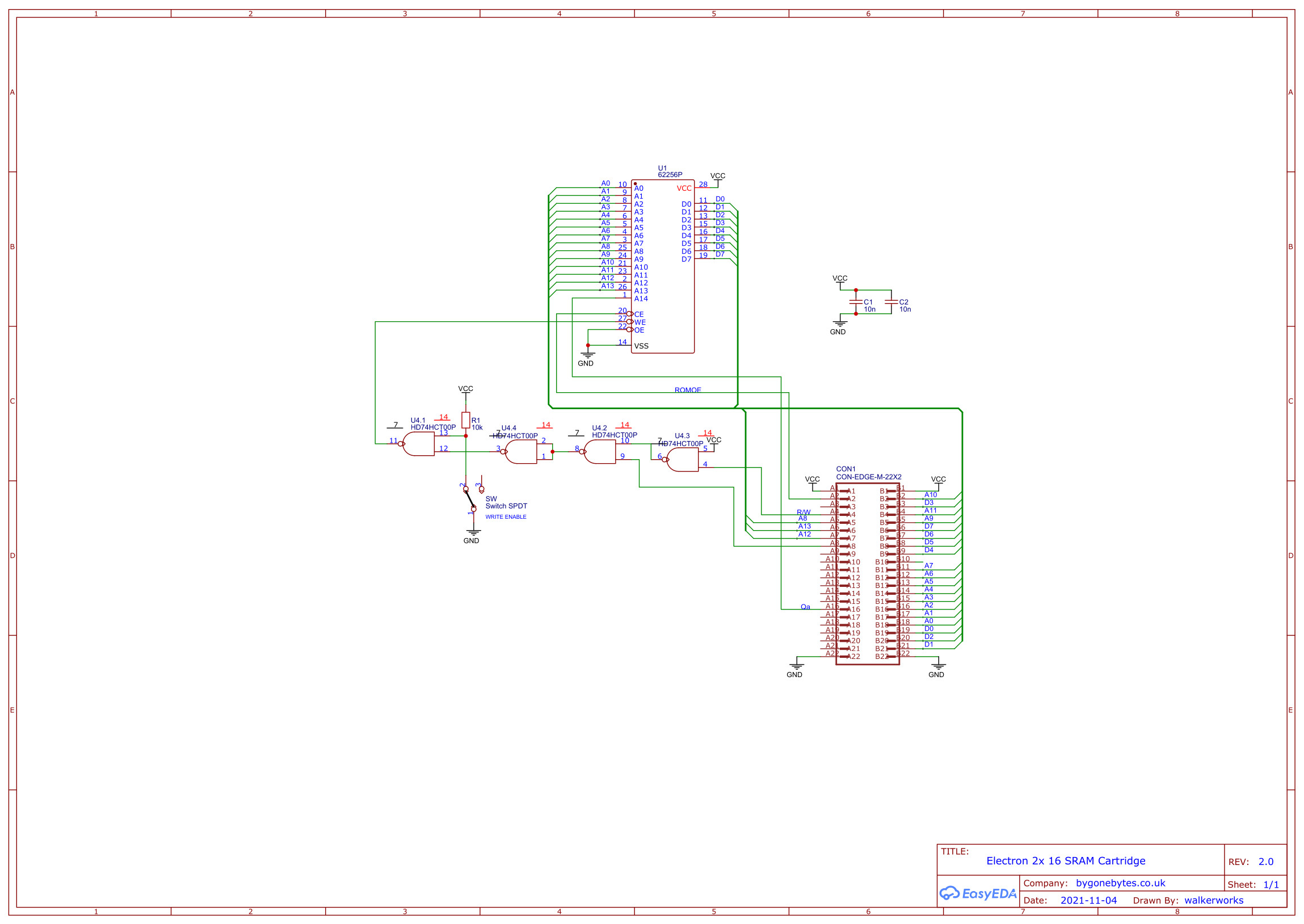
New schematic.

PCB layout.
I modified a v1 board to test the new circuit and can be seen working very reliably.


The modified board under test/

The screen shows RAM present in both banks, both banks loaded and finally both banks write protected.
Potentially something for another revision - after looking at the cartridge edge connector pin-out I noticed there is a third Output Enable available, OE3, that can be used to select ROM 13 (D). I did a quick swap on my test cartridge and yes it does. There is now potential to either add the second RAM chip back onto the board giving three Sideways RAM banks or add a single ROM Socket giving two sideways RAM banks + one sideways ROM bank.


A quick change of two wires and RAM bank 13 (D) appears.


Back to the simplified SRAM cartridge and the PCB is assembled, there's not a lot to it now with only two IC's, two capacitors, one resistor and a switch.

It's a neat little cartridge and works very well. In the picture above I'm using the Minus 1 with the ROM images loaded into ROM positions 4 and 5.

and in this picture I'm using the Plus 1/AP6 combination with the ROM images loaded into ROM positions 2 and 3.
If you would like to build one for yourself everything you need including the Gerbers, BOM and Circuit Diagram are here v2 Electron 2x16K SRAM.